


Hydrogen & Semiconductor Materials
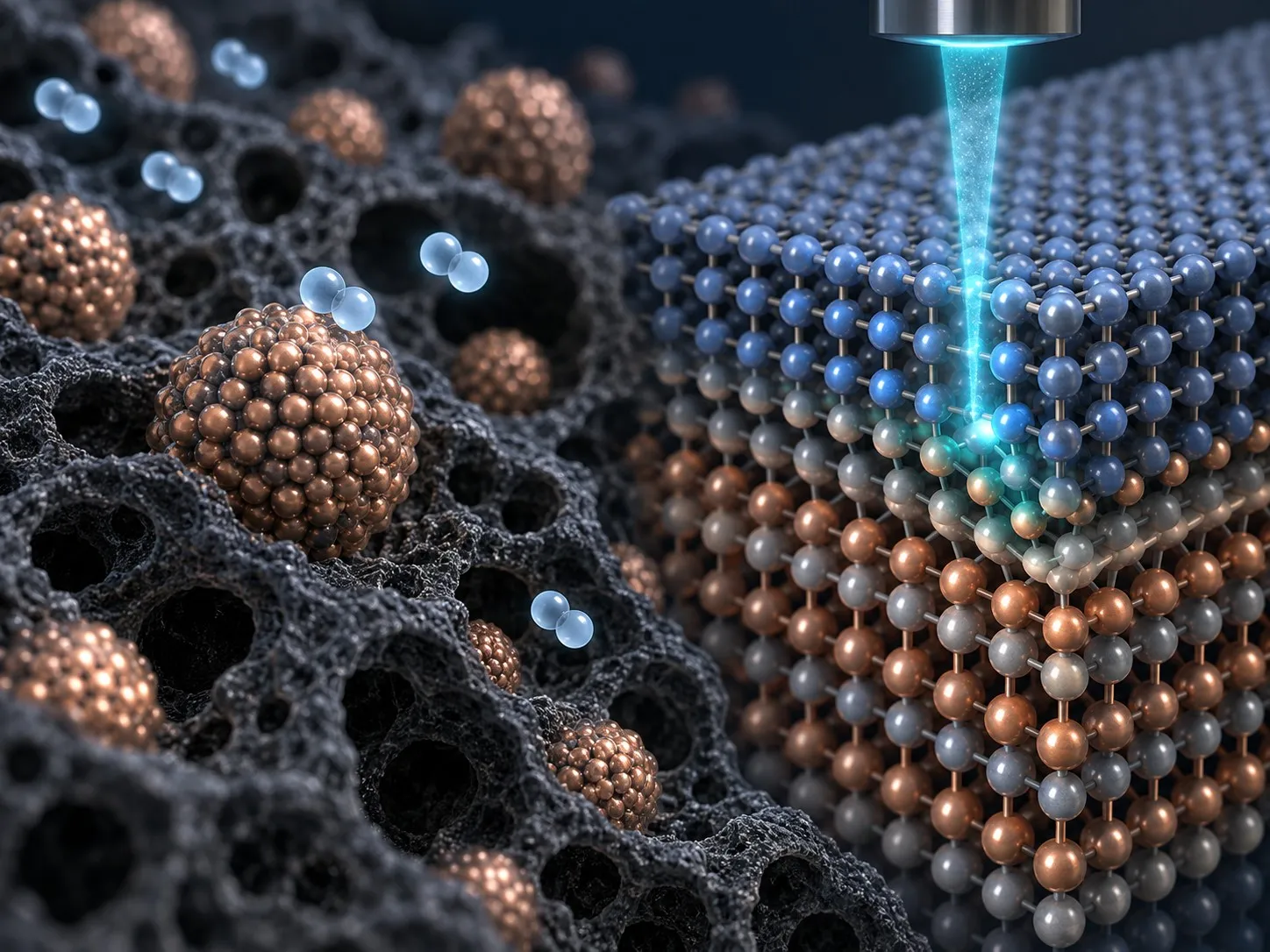
The performance of a catalyst or semiconductor can be shaped by changes confined to a few atomic layers. We extend our microscopy expertise to hydrogen production and fuel-cell catalysts, as well as semiconductor interfaces where defects, strain, and local electric fields govern function. Imaging, diffraction, and spectroscopy connect atomic arrangements with chemical and electronic structure. Through gas-cell experiments, 4D-STEM, and monochromated EELS, we are developing ways to reveal why materials activate, degrade, or change their properties under working conditions.
Hydrogen: understanding catalysts as they work
Catalytic activity depends on the structure of the active surface and its interaction with the surrounding gas. We investigate particle evolution, catalyst–support interfaces, and carbon formation in materials for hydrogen production and fuel cells.
Our gas-cell research connects controlled gas exposure and heating with electron microscopy. Methane pyrolysis for turquoise hydrogen and the evolution of fuel-cell catalysts are key directions. Combining dynamic imaging with 4D-STEM and EELS will help link structural transformations to strain and chemical changes.
A central question is which changes accompany activation and which lead to lasting degradation. We aim to relate particle reshaping, support interactions, and carbon accumulation to the local reaction environment. Following the same particles as conditions change can reveal pathways that are difficult to reconstruct from separate before-and-after specimens.
Hydrogen at the atomic scale
Published examples show how advanced microscopy makes hydrogen-related changes visible—from hydrogen columns at a metal–hydride interface to the lattice strain of a nanoparticle under gas.
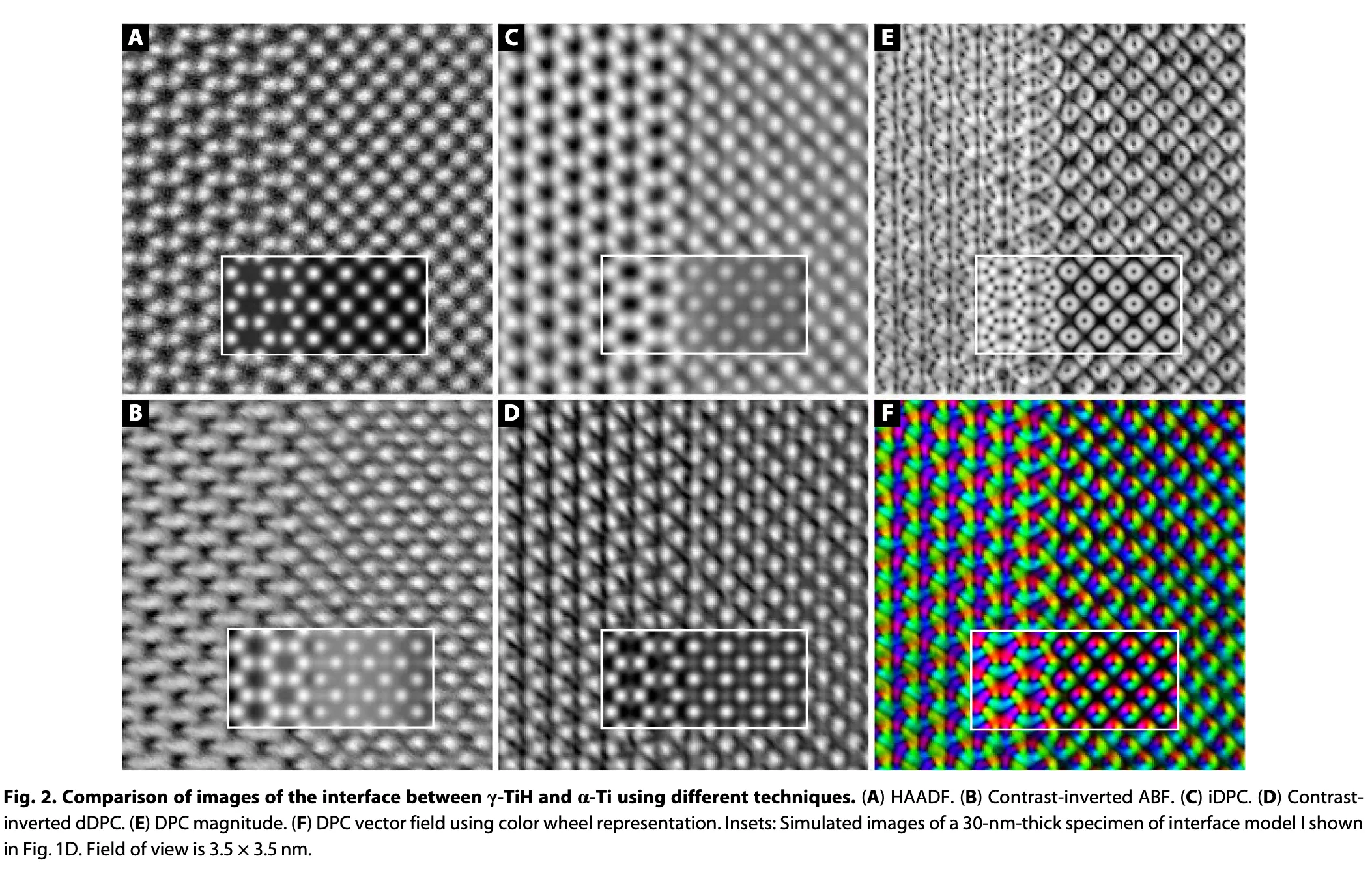
Locating hydrogen columns with iDPC-STEM. Literature example · de Graaf et al., Science Advances (2020), Fig. 2 · Paper · CC BY-NC 4.0
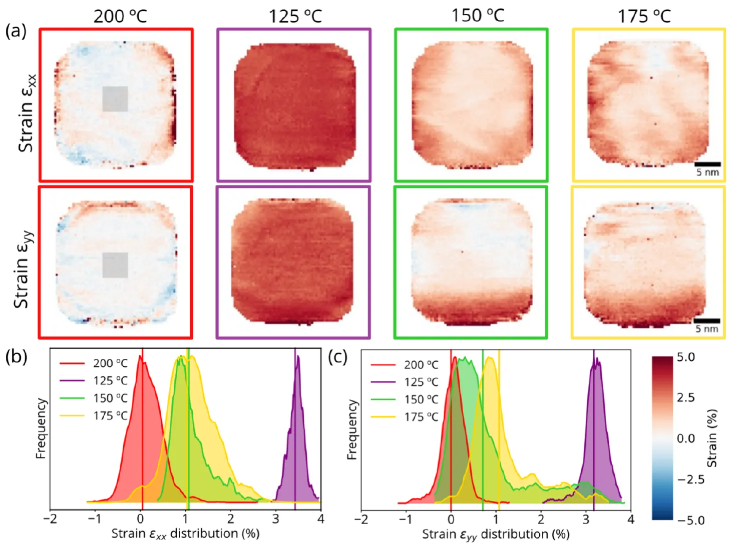
Following lattice expansion and relaxation under hydrogen. Literature example · Perxés Perich et al., Nano Letters (2025), Fig. 4 · Paper · CC BY 4.0
Semiconductors: from atomic interfaces to local properties
At a semiconductor interface, local bonding, defects, and strain can influence device behavior. We combine atomic-resolution imaging, DPC / iDPC, and monochromated EELS to connect these local features with electric fields and vibrational responses.
The aim is to identify where functional behavior originates and how processing changes it—providing a microscopic basis for interface engineering.
An interface may be only a few atomic layers thick, yet differences in atomic arrangement or local bonding can alter polarization and energy transport. We use structural imaging to locate these regions and spectroscopy or diffraction to examine their properties. The combination helps frame questions about how deposition, annealing, and interfacial reactions reshape the functional region of a device.
Structure and vibrations at interfaces
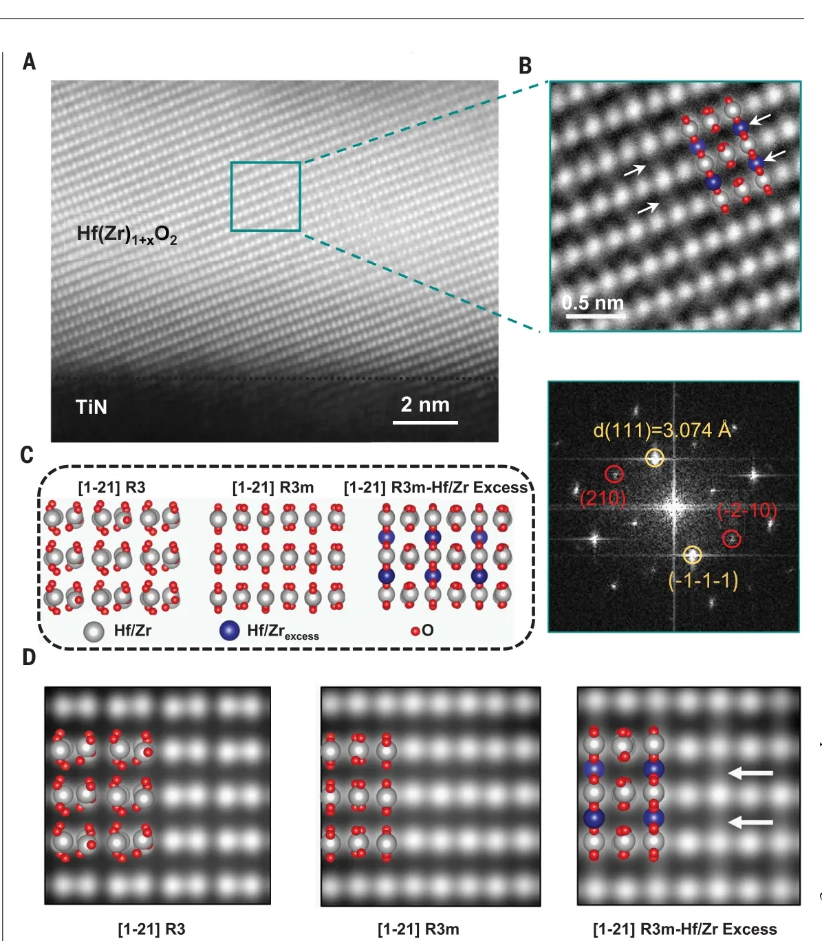
Identifying the atomic structure of a ferroelectric device. Literature example · Wang et al., Science (2023) · Paper
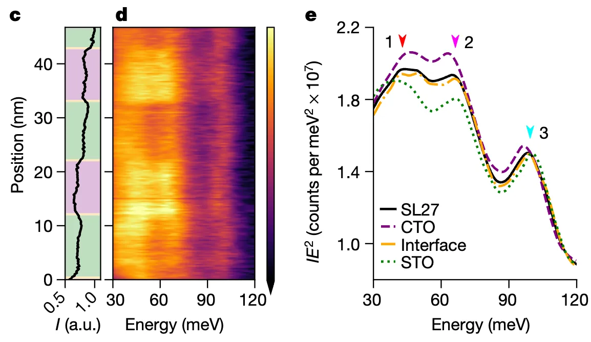
Resolving how lattice vibrations change at an interface. Literature example · Hoglund et al., Nature (2022), Fig. 3c–e · Paper · CC BY 4.0
Connecting materials questions with advanced microscopy
From catalyst activation to semiconductor interfaces, the question determines the experiment. We connect specimen preparation, imaging, diffraction, and spectroscopy around the same region to build a coherent view of material behavior.
Gas atmosphere, temperature, electron dose, and specimen preparation all shape what can be measured. We design observations around these conditions and connect complementary signals so that a visible change can be interpreted in its physical and chemical context. Collaboration begins with defining the reaction or interface that controls performance and selecting the information needed to understand it.
Related research
- Molten GaBi catalyst for low-carbon, cost-effective hydrogen via moderate-temperature methane pyrolysis, Chemical Engineering Journal (2026).
- In situ reaction imaging and analysis