Back to Facilities
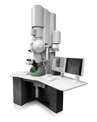
Tecnai G2 F20
TEM ActiveThermo Fisher Scientific — Tecnai G2 F20
Field-emission TEM for general-purpose imaging and diffraction analysis.
Voltage 80/120/200 kV
Gun S-FEG
Monochromator N/A
Pole-piece S-twin (5.4 mm)
EDS Oxford Ultim-Max TLE (0.5-1.1 sr)
Camera Gatan Rio16 CMOS
Accessories Nanomegas ASTAR, TOPSPIN
On this page
Overview
The Thermo Fisher Scientific Tecnai G2 F20 is a field-emission TEM designed for general-purpose imaging, diffraction, and analytical work. Equipped with an Oxford Ultim-Max TLE EDS detector and Nanomegas ASTAR/TOPSPIN systems, it supports a broad range of materials characterization tasks from conventional TEM imaging to automated crystal orientation mapping.
Key Features
- S-FEG electron source: Schottky field-emission gun providing stable, high-brightness illumination
- Oxford Ultim-Max TLE EDS (0.5–1.1 sr): Large solid-angle EDS for efficient elemental analysis
- Gatan Rio16 CMOS camera: High-resolution digital imaging for TEM and diffraction
- Nanomegas ASTAR: Automated crystal orientation and phase mapping via precession electron diffraction
- Nanomegas TOPSPIN: Strain mapping at the nanoscale through nanobeam diffraction analysis
- Multi-voltage operation: 80, 120, and 200 kV for flexible imaging conditions
Applications
- General-purpose TEM imaging and selected area electron diffraction (SAED)
- EDS compositional analysis of thin-film and bulk specimens
- Crystal orientation mapping via precession electron diffraction (ASTAR)
- Nanoscale strain analysis using TOPSPIN
- Routine materials characterization for metals, oxides, and semiconductors