


Back to Facilities
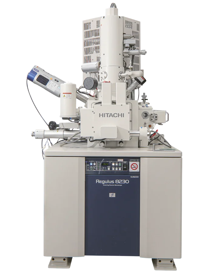
Product image: KIST Advanced Analysis & Data Center · Instrument Catalog
Hitachi Regulus8230
SEM ActiveHitachi High-Tech — Regulus8230
Cold field-emission SEM for low-voltage, high-resolution observation of surface morphology and microstructures in particles, electrodes, and functional materials.
Type Cold field-emission SEM
Electron Gun Cold FEG
Resolution 0.7 nm @ 15 kV
Voltage 0.5–30 kV
Low-voltage Resolution 0.9 nm @ 1 kV (deceleration mode)
Magnification 20–2,000,000×
Stage 5-axis motorized
Overview
Regulus8230 uses a cold field-emission electron source for high-resolution imaging at low accelerating voltages. It supports observation of fine surface features in particles and functional materials, helping connect local morphology with the microstructure of a larger specimen.
Key Features
- Cold field emission: a bright electron source supports fine-probe imaging of nanoscale features.
- Low-voltage observation: emphasizes near-surface information for examining coatings, fine particles, and surface texture.
- Wide magnification range: connects an overview of the specimen with detailed observations of selected regions.
Applications
Particle size and morphology; electrode surface and cross-sectional microstructures; fine features in catalyst and semiconductor materials.
Manufacturer specifications (Regulus series launch specifications)